mbeaudoi
Nanofab Accelerator Program
We are pleased to announce that QMI’s Advanced Nanofabrication Facility (ANF) has just officially launched its Nanofab Accelerator Program in partnership with the National Research Council of Canada Industrial Research Assistance Program (NRC-IRAP). The program will provide eligible SMEs (small or medium-sized businesses) with specialized nanofabrication services, including but not limited to, maskless photolithography, 100kV […]
Flexible Polymer-based Capacitive Micromachined Ultrasound Transducers (polyCMUTs): Fabrication and Characterization
Amirhossein Omidvar, Carlos D Gerardo, Robert Rohling, Edmond Cretu, Antony J Hodgson Conventional ultrasound (US) probes are rigid. The rigidity has several drawbacks including acoustic energy loss and artifacts (due to interface mismatch between skin and probe), patient discomfort, limited field of view, and operator dependency. Many of these problems could potentially be addressed […]
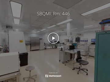
Virtual 3D of the SBQMI/AMPEL ANF Cleanrooms
Main Nanofab Cleanrooms consisting of: ISO 5 (class 100) yellow room ISO 6 (class 1000) yellow room ISO 6 (class 1000) white room Electron Beam Lithography Cleanroom ISO 7 (class 10000) white room JEOL JBX-8100FX 100kV Electron Beam Lithography System Packaging/Workhorse Processes Room […]
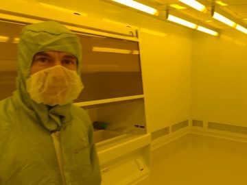
The new SBQMI Nanofab cleanroom
Renovated Cleanroom The facility’s cleanroom is contained within Labs 446 in Brimacombe’s AMPEL wing, and the available floor area is obviously limited by the overall room footprint. In the old configuration, a considerable part of this area was taken by so-called gray space, housing, among other things, vacuum systems, process gases, and other support infrastructure. […]
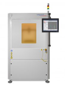
Vanguard Photonic Wire Bonding Tool
The SBQMI now has a photonic wire bonding tool:
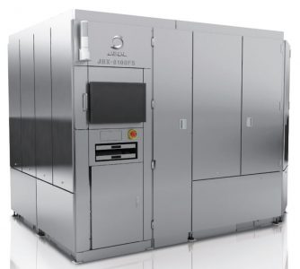
JEOL JBX-81OOFS ELECTRON-BEAM LITHOGRAPHY SYSTEM
SBQMI has invested heavily on acquiring a state-of-the-art electron-beam lithography tool that enables device fabrication at the nanoscale, where quantum properties of materials manifest themselves. An intense, well formed and focused beam of electrons, scanned by precision electronics and driven by computer design data, can directly write features of a few nanometers in size on […]
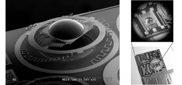
ACTUATED SCANNING MICROLENS FOR NIR RAMAN SPECTROSCOPY
Chin-Pang-Billy Siu and Mu Chiao Dept of Mechanical Engineering, The University of British Columbia, Canada Haishan Zeng, BC Cancer Agency, Canada This paper presents the design, fabrication and characterization of a magnetically actuated scanning microlens for miniature confocal Near Infrared (NIR) Raman spectroscopy. One of the potential applications could be on non-invasive skin cancer […]
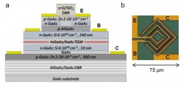
Room-temperature operation of a transistor vertical-cavity surface-emitting laser
X. Yu, Y. Xiang, J. Berggren, T. Zabel, M. Hammar, N.Akram, W. Shi and L. Chrostowski We demonstrate the first room-temperature operation of a transistor vertical-cavity surface-emitting laser (T-VCSEL). Fabricated using an epitaxial regrowth process, the T-VCSEL is electrically a Pnp-type bipolar junction transistor and consists of an undoped AlGaAs/GaAs bottom DBR, an InGaAs triple-quantum-well […]