Current Equipment Status
(last update: June 24, 2025)
| Equipment Name | Current Status | Notes |
|---|---|---|
| AJA evaporator/sputter | Online |
Opened for PM and refilling |
| DeeDirectors evaporator | Online | Room 449 – 8 materials including Au, Cr, Ti, Al, Ni – (Pd, Pt, SiO2, Ge, Ag) |
| NxQ4006 aligner | Online | Please remember to turn off nitrogen |
| Heidelberg MLA150 maskless | Online | Contact Matthias for training/access (should be back week of May 23) |
| JEOL JBX 8100FS Ebeam Lithography System | Online | Room 65; |
| Oxford ICP etcher | Online | restricted to shallow Si etching; |
| Samco RIE etcher | Online | Restricted use to be discussed with ANF staff |
| ECR etcher | Online | Room 449 – turned off but in working order |
| Xactix XeF2 etcher | Online | For selective etching of Si |
| PE-50 plasma asher | Online | |
| Trion PECVD | Online | For SiN and SiO2 deposition & CF4/O2 etching |
| Vanguard Photonics PWB tool | Online | Optical waveguides to interface fibers with photonic devices & circuits |
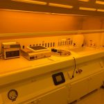
| Wetbench ISO-6 white room | Online | Only bench for dangerous processes; also for processes that don’t require yellow light |
| Wetbench ISO-5 yellow room | Online |
Reserved for EBL processes |
| 200 mm Headway spinner | Online | Reserved for EBL resists only |
| Wetbench ISO-6 yellow room | Online | Photolithography processes only |
| Headway spinner | Online |
Reserved for “regular type” resists |
| Laurell spinner | Online | To be taken out of wetbench after every use. Restricted to special processes |
| Dektak XT profilometer | Online | |
| Nanosurf/Surfscan Atomic Force Microscope | Online | Current tips for use in tapping mode |
| Filmetrics reflectometer F40 | Offline | New F40 unit with microscope & camera – off for repairs |
| 4 point probe | Online | |
| Microscopes with CCD cameras | Online | Now one microscope per room |
| Annealsys Rapid Thermal Anneal | Online | Contact Mario for training |
| MTI muffle furnace | Online | Room 449 |
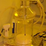
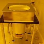
| Miele glassware washer | Online | Use by ANF personnel only |
| Agilent leak detector | Online | For use by ANF personnel only |
| Tresky Die Bonder | Online | Room 449: Use by ANF & SiEPICfab personnel only – waiting on spare temperature sensor. |
| TPT wire bonder | Online | Room 449: Use by ANF & SiEPICfab personnel only |
| DAD3240 dicing saw | Online | Room 449: Use by ANF personnel only |
| MSL: Litho room | Online | MSL NCE 339 – standard lithography room |
| MSL: Soft Litho room | Online | MSL NCE 339 – soft lithography room |
| MSL Parylene Coater | Online | MSL NCE 339 – middle room |
| MSL Vacuum Oven | Online | MSL NCE 339 – standard lithography room |
| QMI: XPS system | Online | Room 344 – training restricted |
| QMI: SEM microscope | Online | Room 273 – training restricted |
| QMI: Ellipsometer | Online | Room 273 – training restricted |
 Wet Chemistry/Wetbench SOP
 Reservation
Optical lithography
SBQMI nanofab is equipped for both contact (physical glass-mask) and maskless (software mask) photolithography. The former is supported by a Neutronix-Quintel model NXQ4006 mask-aligner with a 350W high-pressure mercury lamp, housed in the Class ISO-6 yellow room within the recently renovated cleanroom space, and the latter is supported by the industry-standard Heidelberg model MLA150 maskless tool with laser UV source, housed in the Class ISO-5 yellow room. An extracted wet bench, hot-plates and spinners, situated within the Class ISO-6 yellow cleanroom are also dedicated to photolithography. A wide range of positive and negative resists are supported, including SU-8. The facility has been also recently equipped with two Nikon optical microscopes with camera and metrology capability used for inspection that can be found in the cleanroom.
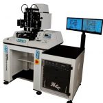
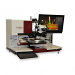
 JEOL JBX-8100FS Electron-beam lithography system
JBX-8100FS 100kV EBL tool capable of writing features as small as 5nm on wafers up to 200mm.
Location: Brim65 (basement of new wing)
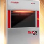 MLA150 Heidelberg maskless lithography system
Location: ISO-5 yellow room
The Heidelberg MLA150 maskless lithography system allows fast direct writing of patterns as precise as 1 micron. It can write on samples as small as 1×1 cm and up to 200 mm wafers.
 NxQ4006: 100 mm mask (currently single side) aligner
Location: ISO-6 yellow room
This mask aligner is a mostly manual system that accepts pieces as small as 7x7mm and wafers up to 100mm diameter. It accepts mask plates 5″x5″ (125x125mm) with the main mask holder but has a holder that can accept mask plates as small as 3″x3″ (75x75mm). It’s optics delivers both 365nm and 405nm light. It is very easy to use for alignment. Although expandable to allow double-side alignment, it does not currently have the adapter to allow it.
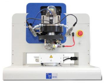
 Vanguard Photonic Wirebonder
Location: ISO 6 Yellow room
This tool allows 3D, 2 photon lithography. It’s main purpose is to create waveguides to mate different photonic circuits together.
 HEADWAY PWM50: 200mm resist spinner
Location: ISO-5 yellow room wetbench
Currently reserved for spinning of Electron Beam Resists only. The spinner can accommodate wafers up to 200mm diameter.
 HEADWAY PWM32: Photoresist spinner
Location: ISO-6 yellow room
Currently reserved for spinning of traditional photoresists such as AZ5214, S1813, etc.
This programmable spinner allows spinning various photoresists on wafers of various sizes. The maximum size wafer that can be accommodated by this spinner is a 6″ wafer. See video on how to install the aluminum foil.
 LAURELL WS-400-6NPP-LITE: Photoresist spinner
Location: currently offline
This programmable spinner allows spinning of various photoresists on wafers of various sizes. The maximum size wafer that can be accommodated by this spinner is a 6″ wafer.
Thin Film Deposition
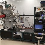
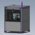
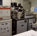
AJA UHV Ebeam and Sputter Evaporator
AJA UHV Hybrid Evaporator
Location: ISO-6 white room
The SBQMI Nanofabrication Facility has an AJA load-locked, ultra-high-vacuum (UHV), hybrid deposition system. It is dedicated to high-purity evaporation of non-magnetic materials.
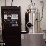 DEEDIRECTORS2015: 8 source load-lock electron beam evaporator
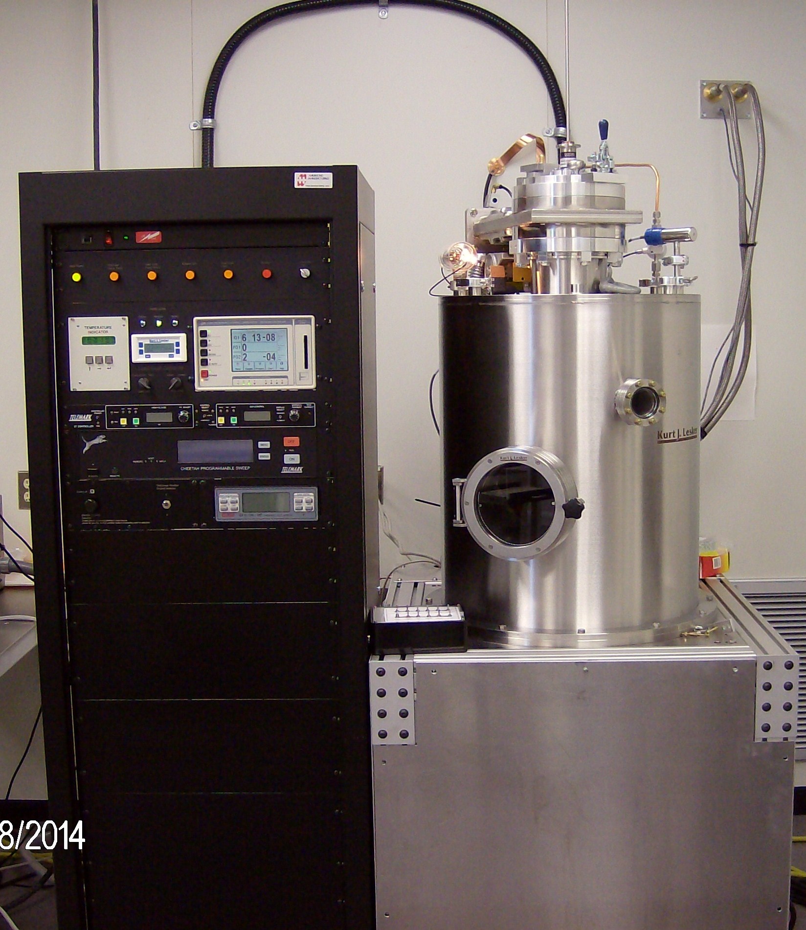
Location: Brim449
This is a high vacuum system expected to come online sometime in 2014. In this system, up to six various materials can be evaporated in a single process. A load-lock will allows samples to be loaded without exposing the main chamber to air thus greatly reducing pumpdown time. The film thickness is controlled during evaporation with a thickness monitor.
 TRION: PECVD/RIE system
Location: ISO-6 white room
 POS Labcoter: Parylene Coater
Location: MSL room NCE 339
Plasma & Dry Etching
Oxford COBRA: ICP plasma etcher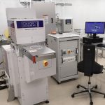
Location: ISO-6 white room
This system uses C4F8, O2, SF6 and Ar chemistries. It is dedicated to shallow silicon etching.
Samco RIE 10-NR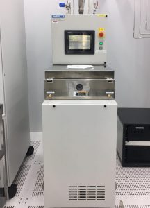
Location: ISO-6 white room
This system uses CF4, CHF3, O2, SF6 and Ar chemistries. It is dedicated to etching of superconducting metals. Other materials may be allowed in the system upon discussion with ANF staff.
 PLASMAQUEST: ECR plasma etcher
Location: Brim449
This system uses CF4, CHF3, O2 and Ar chemistries. It is used extensively to etch SOI and GaAs based photonic nanocrystals, GaAs based VCSELs as well as various other materials.
 Plasma-Etch PE-50: Plasma etcher
Location: ISO-6 white room
The system uses Ar and O2 gases. It can be used for descum, or total removal of photoresist.
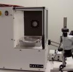 XACTIX: XeF2 etcher
Location: ISO-6 white room
This is a dry etching system. It uses Xenon Difluoride for isotropic Silicon etch.
TRION: RIE/PECVD system
Location: ISO-6 white room
This system uses di-ethyl silane (DES), NH3, N2, N2O and has been optimized for the PECVD deposition of Si3N4 and SiO2. However, it can also be used as an RIE etcher for these materials with CF4/O2 chemistry as well as for O2 ashing/descum.
Thermal treatment
 Annealsys AS-ONE RTP system
Rapid Thermal Processing (RTP) system capable of ramping T up to 1200C under various atmospheres: air, nitrogen, argon or forming gas.
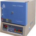 KSL 1100X: Box Furnace
Box (muffle) furnace used for bonding or other thermal treatments. In room 449.
Metrology
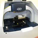
FILMETRIX F40: Thin film thickness measurement system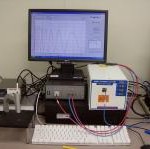
Location: ISO-6 yellow room
This instrument is used to measure the thickness of transparent and semi-transparent thin films via reflection or transmission spectroscopy. Films as thin as a few tens of nm can be measured when the UV light is turned on. An SOP will be coming soon.
Nikon: Microscopes with CCD camera
Location: 1 in each of the yellow rooms
This microscope can image in bright/dark fields. It can be used for simple imaging and also does Nomarski microscopy. Image capture is via a CCD camera.
ZEISS: Microscope with CCD camera 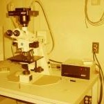
Location: ISO-6 white room
This microscope can image in bright/dark fields. It can be used for simple imaging and also does Nomarski microscopy. Image capture is via a CCD camera.
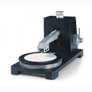
 DEKTAK XT: Profilometer with 3D capability
Location: ISO-6 white room
This semiautomatic profilometer can be used for single and multiple scans. It provides data on a film thickness, or on a surface roughness and also allows 3D visualization of the scanned structures. It can moreover be used to measure stress of thin films.
 EverBeing SR-4, Sheet Resistivity, 4-Point Probe
Location: ISO-6 white room
This 4 point probe can be used to measure the resistivity of various films.
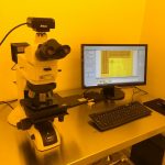
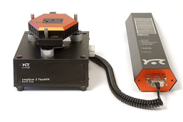 Easy Scan 2 Atomic Force Microscope
Location: ISO-6 white room
This student level AFM microscope is easy to use and generates nice images. It currently has tips for tapping mode measurements but other tips can be purchased.
Packaging
 Tresky Die Bonder
Location: Brim 449, ISO-7 cleanroom
This tool allows bonding of small die onto a chip or carrier. It is currently used to attach laser diodes to silicon photonic chips.
 TPT Wirebonder
Location: Brim 449, ISO-7 cleanroom
This tool allows wirebonding of die and chips onto carriers.
 Disco DAD3240 Dicing Saw
Location: Brim 449 normal room
This tool allows dicing of wafers into small die for further packaging. This dicing saw is able to dice wafers up to 200 mm diameter. It can dice several materials ranging from semiconductor wafers to ceramics and other substrates. Discuss with ANF staff to determine if it can server your needs.
Work is performed by ANF operators with exceptions allowable for heavy users.
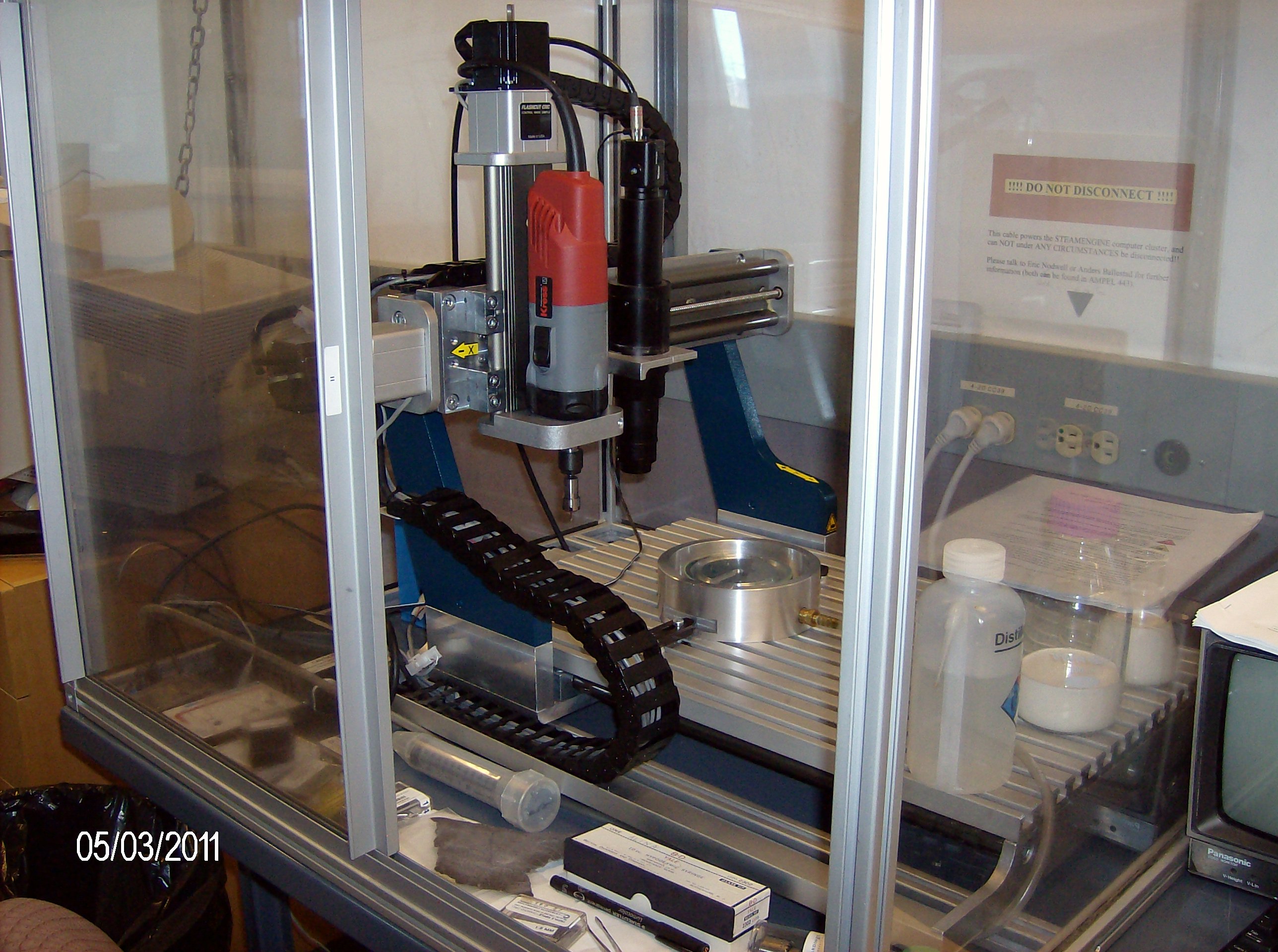 CNC microdrill
Location: AMPEL/SBQMI machine shop
Currently offline but located in SBQMI machine shop. This drill was used in the past to drill small holes into glass slides to serve as access to microfluidics chips.