The University of British Columbia
UBC - A Place of Mind
The University of British Columbia Vancouver campus
AMPEL Advanced Nanofabrication Facility (ANF)
  • Home
  • Facility: Access and Info
    • Becoming a member
    • Fee structure
    • ANF Store
    • Webcams
  • Equipment
    • Equipment Reservation
    • Wetbench SOP
    • Analysis
      • FILMETRIX F20: Thin film thickness measurement system
      • ZEISS: Microscope with CCD camera
      • DEKTAK XT: Profilometer with 3D capability and imaging
      • ALPHA STEP 200: Profilometer
    • Etching
      • PLASMAQUEST: ECR plasma etcher
      • Plasma Etch PE-50 Plasma etcher/cleaner
      • XACTIX: XeF2 etcher
    • Thin Film Deposition
      • TRION: PECVD & RIE
      • DEEWONG-2000: 4 sources electron beam evaporator
      • DEEDIRECTORS-2015: 8 source load-lock electron beam evaporator
      • AIRCO TEMESCAL: Dual 3in source RF magnetron sputter system
      • AJA Hybrid Evaporator System
    • Lithography
      • CANON PLA-501F: Double Side Mask Aligner
      • Neutronix-Quintel NxQ4006: 100mm mask aligner
      • HEADWAY PMW32: Photoresist spinner
      • LAURELL WS-400-6NPP-LITE: Photoresist spinner
    • Furnaces
      • KSL-1100X: Box furnace
      • LINDBERG: Tube furnace
      • MINIBRUTE: Tube furnace
      • HEATPULSE 210: Rapid thermal anneal (RTA) system
    • Other
  • Processes
    • Lithography
      • AZ P4110 Process
      • AZ 4620 process
      • Silicone Rubber Micromolds (PDMS)
    • Thin film deposition
      • PECVD of SiNx and SiO2
    • Cleaning and wet etching
      • Si wafer cleaning
      • RCA-1 Si wafer cleaning
      • RCA-2 Si wafer cleaning
      • Piranha etch
      • BOE (Buffered Oxide Etch) and HF dip
      • Si anisotropic etch (KOH, TMAH)
      • Si Isotropic etch (HNA)
      • Glass substrate cleaning
      • Glass wet etching
      • Gold Etch Using Potassium Iodide Solution
    • Plasma processes
    • Processing links and resources
  • Education
  • SAFETY
  • People
    • Kostis Michelakis
    • Mario Beaudoin
    • Andrey Blednov
    • Lukas Chrostowski
    • Josh Folk
    • Alina Kulpa
    • Jim Mackenzie
    • ANF Users
  • AMPEL
  • Cleanroom Renovations
  • Contact us
  • Renovations News and Equipment Status

    During the cleanroom renovations, we have tried to keep the most common processes available.  

  • JEOL JBX-81OOFS ELECTRON-BEAM LITHOGRAPHY SYSTEM

    SBQMI has invested heavily on acquiring a state-of-the-art electron-beam lithography tool that enables device fabrication at the nanoscale, where quantum properties of materials manifest themselves. An intense, well formed and focused beam of electrons, scanned by precision electronics and driven by computer design data, can directly write features of a few nanometers in size on […]

  • ACTUATED SCANNING MICROLENS FOR NIR RAMAN SPECTROSCOPY

    Chin-Pang-Billy Siu and Mu Chiao Dept of Mechanical Engineering, The University of British Columbia, Canada Haishan Zeng, BC Cancer Agency, Canada   This paper presents the design, fabrication and characterization of a magnetically actuated scanning microlens for miniature confocal Near Infrared (NIR) Raman spectroscopy. One of the potential applications could be on non-invasive skin cancer […]

  • Room-temperature operation of a transistor vertical-cavity surface-emitting laser

    X. Yu, Y. Xiang, J. Berggren, T. Zabel, M. Hammar, N.Akram, W. Shi and L. Chrostowski We demonstrate the first room-temperature operation of a transistor vertical-cavity surface-emitting laser (T-VCSEL). Fabricated using an epitaxial regrowth process, the T-VCSEL is electrically a Pnp-type bipolar junction transistor and consists of an undoped AlGaAs/GaAs bottom DBR, an InGaAs triple-quantum-well […]

  • Ebeam lithography for nanometer scale devices

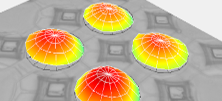
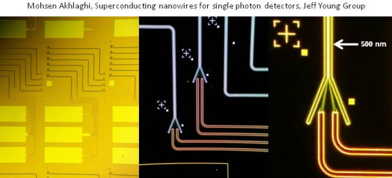
The Nanofab is the center for device fabrication at UBC for multidisciplinary applications including microfabrication of microfluidics devices (for proteomics, DNA sequencing, lab-on-chip, cell cultures), photonics (photonic crystals, lasers, modulators), and nano-electronics (carbon nanotube devices, graphene electronics).
The facility is used by research groups from the faculties of Applied Science, Science and Dentistry, as well as off-campus academic and industrial users.

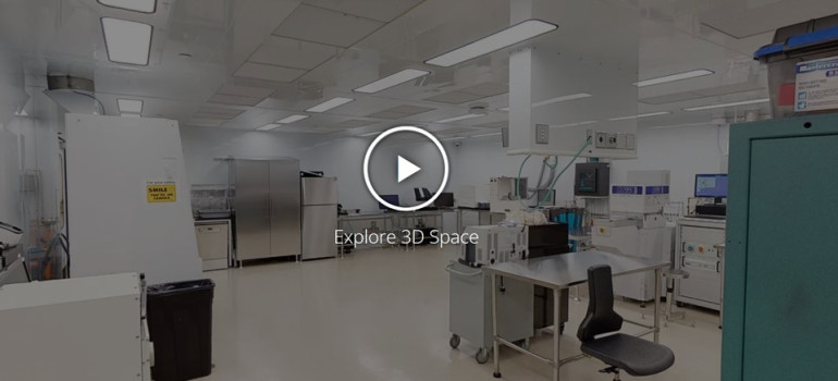
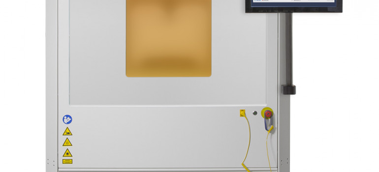
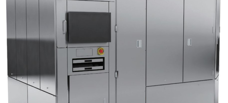
The Nanofabrication Facility is a cleanroom laboratory situated on the fourth floor of the AMPEL building.

The AMPEL Nanofabrication Facility is a fee-based laboratory open to UBC and outside users, as a service, or for trained users. As a service laboratory in Vancouver, our experienced process staff are available to perform fabrication tasks ranging from single steps to full device fabrication. To gain access to the facility and for any other enquiries, please contact the manager, Mario Beaudoin, at 604-822-1853 or anf “at” ampel.ubc.ca. You can also get in touch with the director(s) at nanofab “at” ampel.ubc.ca.

Equipment reservations are made through Bumblebee …

  • News
  • Equipment Status


All equipment are currently up and running. During the upcoming renovations, we will keep a list of the available equipment, in alternate rooms, as well as alternative possibilities for our offline equipment.

Ebeam lithography will not be affected by the cleanroom renovations while traditional wetbench and photolithograpy processes will be available in AMPEL 442.

Equipment will still be reserved through the bumblebee reservation system: Bumblebee but there will not be a need to sign-in; the charges will be calculated per equipment reservations and will come out to be approximately the same as current charges.


AMPEL Advanced Nanofabrication Facility
Vancouver Campus
2355 East Mall
Vancouver, BC Canada V6T 1Z4
Tel 604 822 1853
Website www.nanofab.ubc.ca
Email anf@ampel.ubc.ca
Back to top
The University of British Columbia
  • Emergency Procedures |
  • Terms of Use |
  • Copyright |
  • Accessibility