 AZ P4110 Process
To describe the positive photoresist recipe used in the AMPEL Nanofabrication Facility using the AZ P4110 Photoresist and matched AZ 400K developer diluted 1:4. AZ is a trademark of Clariant Corporation.
AZ 5214E-IR Direct and Image Reversal Process
To describe the photoresist recipe used in the AMPEL Nanofabrication Facility using the AZ 5214E-IR photoresist both as a positive photoresist and, with image reversal, as a negative photoresist.
Lift-off process using a bilayer LOR/PMGI and Any Resist
To describe the photoresist recipe used in the SBQMI Nanofabrication Facility using the LOR/PMGI bi-layer process and any other photoresist.
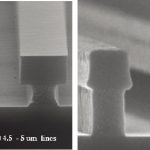
 AZ 4620 Process
The process described here is to deposit thick (12 μm) AZ4620 resist, which can be used as electroplating molds, with good resolution and reproducibility. The patterning of AZ4620 photoresist is performed by using a mask and an UV light contact aligner. This is a level-2 process; it requires superuser instruction.
 Quick MSL recipe for PDMS
Silicone rubber (PDMS) is a stable, high resolution elastomer which can be used make very accurate impressions of micro structures. These reduced instructions are used in the Michael Smith Laboratory’s Soft Lithography room (managed by ANF).
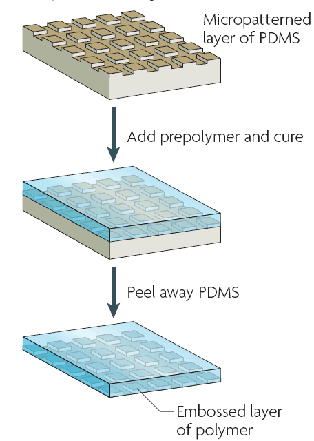
 Silicone rubber micromolds (PDMS)
Silicone rubber (PDMS) is a stable, high resolution elastomer which can be used make very accurate impressions of micro structures. It can be used as a final device or as a mold for making devices out of other polymers. Since it is somewhat compliant and very inert, it makes an ideal molding compound. Silicone can handle temperatures in excess of 300 °C, so it can even be used as a mold for low melting point metals such as tin. This is a level-1 process; it requires general instruction.
Mask Making with MLA-150
This SOP describes the fabrication process of a photomask using the MLA150 inside the UCB cleanroom.