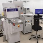
 https://www.nanofab.ubc.ca/equipment/etching-4/oxford-cobra-icp-etcher/
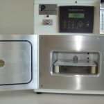
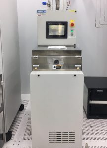 https://www.nanofab.ubc.ca/equipment/etching-4/samco-rie-10nr/
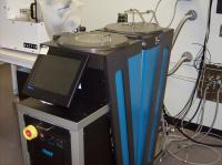 https://www.nanofab.ubc.ca/equipment/thin-film-deposition/trion-rie-pecvd/
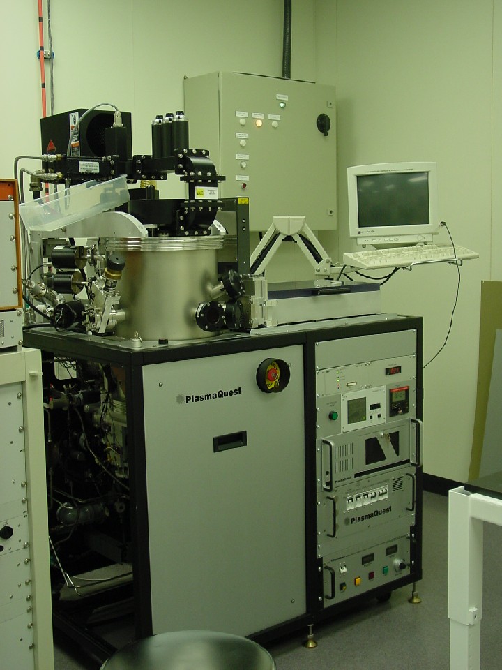
https://www.nanofab.ubc.ca/equipment/etching-4/ecr-etcher/
https://www.nanofab.ubc.ca/equipment/etching-4/pe-50-planar-etcher/
 Handbook of Plasma Processing Technology – Fundamentals, Etching, Deposition, and Surface Interactions